
Remember me
Export citation and abstractBibTeXRIS
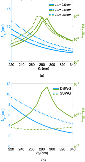
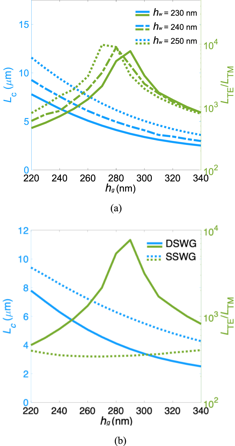
Due to an accidental error, incorrect figures were included in figures 3(b) and 8(b), resulting in figure 3(a) being identical to figures 3(b) and 8(a) being identical to figure 8(b), as reported in the original paper [1]. Figure 3(a) illustrates the device footprint (Lc) and the coupling-length ratio for both TE and TM modes (LTE/LTM) as a function of the DSWG height (hg) for various values of hw. The corrected figure 3(b) (see below) compares the LTM and LTE/LTM values of the DSWG (this study) with those of a single SWG (SSWG) at hw = 230 nm.
Figure 3 (a) Coupling length of TM mode (LTM) and coupling-length ratio (LTE/LTM) as a function of hg of the present DSWG at various values of hw. (b) Comparison of LTM and LTE/LTM between the DSWG and SSWG at hw = 230 nm.
Download figure:
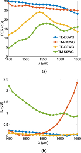
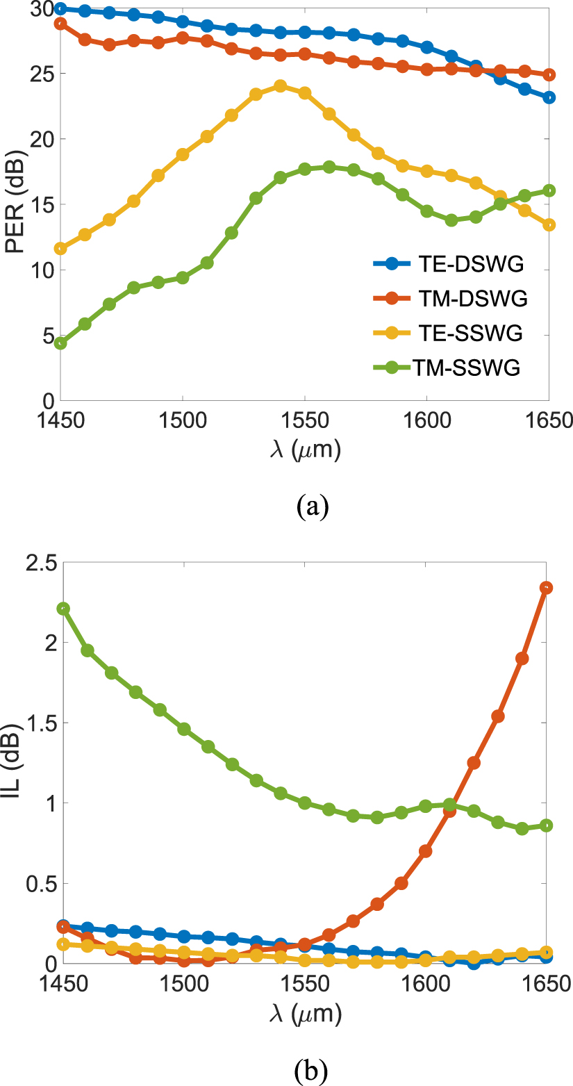
Standard image High-resolution imageFigure 8 (a) The PER and (b) IL as functions of the operating wavelength λ at ρpx = 0.8, ρz = 0.5, wSi = 400 nm, hw = 230 nm, hg = 320 nm, and s = 540 nm.
Download figure:
Standard image High-resolution imageThe original figure 8(a) presents the polarization extinction ratio (PER) of the DSWG and SSWG structures as a function of the operating wavelength. Figure 8(b) shows the insertion loss (IL) of both structures over the same wavelength range, used to evaluate the operational bandwidth (BW). These results are based on the optimized parameters: ρbx= 0.5, ρpx = 0.8, ρz= 0.5, wSi = 400 nm, hw = 230 nm, hg = 320 nm, and s = 540 nm (see below).
Comments (0)