
Remember me
The rapid development of space communication and sensing puts forward high requirements on the performance of systems and devices. Integrated photonics takes advantages of reduced size, weight, and power consumption (SWaP) and provides a high level solution in the fields of space communication and sensing with limited space and payload. This paper reviews the typical applications of integrated photonics in space communication and sensing.
1.1. Introduction to satellite laser communication and space sensingWith the rapid development of satellite remote sensing and the increasing of space activities, real-time transmission of massive data is highly needed. Limited by carrier frequencies, SWaP parameters, and confidentiality, traditional microwave communication is no longer well enough to meet the high-speed and high-capacity communication demand between satellites and ground. Based on the information carrier of laser, free space optical communication takes advantages of high frequencies, good spatial and temporal coherence abilities, small divergence angles, and good directionality. It is an effective way to solve the bottleneck problems of microwave communication. Space-based broadband networks with high-speed and real-time performance between satellites and ground can be built by free space optical communication. This approach can also be used among satellites in various orbits, as well as deep space exploration.
After decades of development, satellite-based laser communication has evolved from on-ground tests to in-orbit experiments. Multiple in-orbit experiments have been completed. The United States began to research space optical communication in the 1960s and 1970s. After the Space Technology Research Vehicle 2 satellite-to-ground lasercom experiment [1], a series of studies were conducted, including the Lunar Laser Communication Demonstration project [2], the Optical Payload for Lasercom Science system [3], and the Laser Communications Relay Demonstration Project [4]. In 2021, laser intersatellite links were constructed among satellites constellations by the Starlink of the SpaceX company of the United States [5]. In the 1990s, the European Space Agency developed an inter-orbit optical communication system called Semiconductor Laser Intersatellite Link Experiment [6]. In 2001, an inter satellite laser communication link was constructed between low earth orbit observation satellites and geosynchronous orbit satellite [7]. In 2008, the German Aerospace Center conducted the first space coherent laser communication [8]. The European Data Relay System (EDRS) known as the SpaceDataHighway was designed to provide commercial data relay service to spacecraft in low earth orbit. EDRS-A, the first orbital node of the system was launched in late 2016. In a second step, EDRS-C, a complete satellite was added in August 2019 [9].
Japan has also made progress in satellite laser communication, such as on-orbit free-space laser communications between the Optical Inter-orbit Communications Engineering Test Satellite and the Advanced Relay and Technology Mission geostationary satellite [10] and the Small Optical TrAnsponder for micro-satellites [11]. The Japan Aerospace Exploration Agency launched a new data relay satellite with optical inter-satellite communication technology in 2020 successfully [12].
China started relatively late, but developed rapidly in the field of space optical communication. In November 2011, optical communication was established between the low orbit satellite HY-2 and the ground [13]. In 2016, a low orbit satellite to ground coherent laser communication experiment was conducted using the quantum experiment science satellite called Micius [14]. In 2023, China undertook a series of experiments on satellite-to-ground laser communication using the Jilin-1 satellite and achieved a successful throughput of 10 Gbps [15].
As two of typical representatives of space applications, both space communication and sensing are very important. With the rapid development of space technology, satellite-based sensing gradually attracts the attention of public. Space sensing is a kind of non-contact detection technology. Relevant information can be obtained through the interaction between electromagnetic waves and objects. In addition to understand nature, space sensing technology has become an indispensable tool to explore outer space and expand our knowledge of the earth and the universe.
As a representative work in remote sensing, Landsat established by the United States for terrestrial satellite remote sensing was first placed in orbit in 1972. The Landsat system has contributed significantly to understand the environment of the earth, and encouraged a new generation of commercial satellites for regional, high-resolution spatial images [16]. Worldview-1 Launched on 18 September 2007 by Digital Globe Inc. was one of the high-resolution satellites providing stereo scenes for civil use [17]. Launched in 2009, the Lunar Reconnaissance Orbiter of the National Aeronautics and Space Administration (NASA) was implemented to explore the lunar surface and environment at resolutions and over time scales never achieved before [18]. The Landsat 9 launched in 2021 continued to view the world [19]. In 2014, the European Space Agency undertook the development of a European radar observatory (Sentinel-1) to provide routine, day-and-night, all-weather medium resolution observation [20]. Sentinel-3 A and 3B were launched in 2016 and 2018, respectively, and dedicated to water level measurement [21]. The SpEye mission, funded by Italy, was a 6 U CubeSat mission designed to showcase inspection and guidance, navigation, and control capabilities in proximity operations using a nanosatellite. In 2023, the SpEye mission successfully completed phase A by clearing the system requirement review milestone [22]. An imaging and spectroscopy mission project officially started in 2018 at the Japan Aerospace Exploration Agency. The spacecraft was launched in 2023 to perform high-resolution spectroscopy and comprehensive field-of-view imaging [23]. A civilian satellite of China named ZiYuan-3 was launched on 9 January 2012 to provide high-precision data [24]. With the development of BeiDou satellite in 2023, the navigation satellite system can provide high-precision services [25].
1.2. Introduction to integrated photonicsIntegrated photonics concentrates on optoelectronic devices and systems on a single chip. The micro optical system called photonic integrated circuits (PICs) formed by integrating active devices, such as lasers, detectors, and modulators on the same substrate. Passive devices, including optical waveguides, filters, and couplers can be used to connect them. PICs can be widely used in various fields, such as information processing, communication, and sensing for the advantages of high data transmission rates, low costs, universalities and scalability. Optical communication is a main driving factor for the development of commercial PICs. Silicon (Si) photonic chips have been widely used in data communication. In the future, PICs with large-scale integration, high-level performance, and embedded computing ability may be required. In addition to communication, PICs could promote the development of various applications, such as virtual reality, autonomous driving, imaging, and biophotonics.
Various material platforms can be used to fabricate integrated photonics, which mainly including Si-based, Ⅲ/V, and Ⅲ-V/Si hybrid platforms, as well as the emerging thin-film lithium niobate (LiNbO3) platform. Various CMOS compatible platforms, such as Si on insulator (SOI) and silicon nitride (Si3N4) on insulator, can be used to fabricate large-scale integrated devices with low cost. At present, there are no platforms to meet all the required functions of integrated photonics [26–28].
Si-based optoelectronic devices mainly used in the near-infrared band play an important role in PICs. Si3N4 waveguides attract attention for low transmission losses and high input power. For the low index contrasts, Si3N4 devices are stable to phase errors. As one of the Ⅲ–V semiconductor materials, InP is suitable for devices operating in the wavelength range of 1.3–1.6 µm and can be used to fabricate various active and passive devices. Thin film LiNbO3 is highly attractive for various advantages, such as excellent electro-optical performance, a wide transparency window, and a relatively high refractive index.
1.3. Significance of integrated photonics in spaceDiscrete devices usually used in space communication and sensing are large, heavy, and power-hungry. Space devices with compact and integrated solutions are highly needed by the stringent requirements in space with huge demand for high-performance and low-cost modules. Compared to discrete equivalents, PICs take advantages of functionality, SWaP, costs, reliability, scalability, and less sensitive to external perturbations, such as vibrations and temperature gradients. Some integrated devices, such as lasers, modulators, detectors, and optical amplifiers, develop rapidly [29–34], as well as the packaging technology for the devices [35, 36]. The integration of multiple optical components on a single chip is increasing the applications of photonic devices in space communication and sensing. To meet the increasing demand of space resources, integrated photonics can be further used to promote sustainable progress in space technology.
At present, the applications of integrated photonics in space communication and sensing mainly include the following aspects: digital laser communication and microwave photonic chips based on satellites, ranging, imaging, inertial sensing, and material analysis. This review focuses on the applications of integrated photonics in space communication and sensing and is organized as follows. In section 2, applications of integrated photonics in the field of space communication are introduced from digital communication and microwave photonic chips. In section 3, integrated photonics for ranging and imaging are introduced as the typical applications of sensing, as well as inertial sensing and material testing. In section 4, we focus on the performance and reliability challenges faced by integrated photonics in the space environment. The review is then summarized in section 5.
Currently deployed satellite communication mainly relies on radio frequencies. A good explanation and SWaP comparison between RF and optical payloads was provided [37]. For the benefits of increased capacity and improved synchronization accuracy, intersatellite links using free-space optical communication have already been implemented and tested on different orbits for future navigation systems. To meet the needs of high-performance transmission and reception among satellite terminals, it is necessary to develop integrated optoelectronic chips for digital laser communication. Integrated microwave photonic chips are a feasible solution to replace traditional discrete devices [38–40]. In this section, we give an overview of the development of integrated photonics in the field of space communication. It mainly involves Si photonic transmitters and receivers for satellite-based digital laser communication, as well as integrated microwave photonic modulators, oscillators, and filters.
2.1. Satellite-based digital laser communication chipsLarge bandwidths between satellites and/or between satellites and ground stations are highly desirable. Radio frequency systems are limited to enlarge bandwidths, as well as the frequencies regulated by the International Telecommunication Union. For the significant advantages of large capacity, convenient connections, and excellent security, the demand of free-space optical communication systems increases rapidly. Laser communication terminals for satellite constellations are mandatory.
With the rapid development of on-chip integrated lasers, detectors, modulators, optical amplifiers, and other photonic devices, as well as the continuous advancement of optoelectronic packaging, integrated photonics is applied to satellite laser communication. Integrated devices are more powerful, reliable, and scalable than the discrete ones. Compact and low-cost digital laser communication systems can be achieved by integrated devices. Satellite digital laser communication involves the transmission and reception of signals. We will discuss integrated transmitters and receivers in detail in this section.
2.1.1. Integrated transmittersThe function of transmitters in space laser communication systems is to load input signals, such as images and audio signals, onto laser beams, and then transmits modulated optical signals to space through optical antennas.
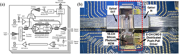
A 40 Gbps optoelectronic transceiver with a high-density integration of optical and electrical components was demonstrated in 2008 [41]. Block diagram of one of the four 10 Gbps transceiver channels is shown in figure 1(a). The 40 Gbps Si transceiver in a quad small form factor pluggable module was supported by the Defense Advanced Research Projects Agency of the United States. The transceiver with a co-packaged externally modulated continuous wave laser was on the verge of becoming the first commercial application [41].
Figure 1 Schematic of integrated transmitters. (a) Block diagram of one of the four 10 Gbps transceiver channels. Reproduced with permission from [41]. (b) Photograph of the 16-channel photonic-electric co-designed Si transmitter. Reproduced with permission from [43].
Download figure:
Standard image High-resolution imageIn 2013, Freedom Photonics in the United States demonstrated the first widely tunable monolithically integrated photonic coherent transmitter in InP based on quantum-well intermixing [42]. Combined with a multimode interferometer-based nested Mach–Zehnder modulator (MZM), a compact device with a footprint of ∼2 mm2 was fabricated. The transmitter incorporating an integrated sampled grating distributed Bragg reflector (SGDBR) laser with a 40 nm tuning range was able to transmit non-return-to-zero (NRZ) quadrature phase-shift-keyed (QPSK) signals at a rate of 20 Gbps [42].
Another InP transmitter developed by University of California, Santa Barbara was proposed for deep space optical communication [44]. The transmitter supported by NASA consisted of a frontend InP PIC followed by an average-power-limited amplifier, and was capable to transmit 16-ary pulse position modulation with a 28-dB extinction ratio [44].
Return-to-zero differential phase shift keying (RZDPSK) is an attractive and efficient format for space optical communication. Under a NASA innovation program, a PIC transmitter for space optical communication utilizing a RZDPSK modulation format was realized on an InP platform. The monolithic InP transmitter generated RZDPSK modulation up to 5 Gbps. Differential phase shift keying and NRZ on–off keying (OOK) modulation up to 10 Gbps was achieved [45]. A transmitter included a widely tunable SGDBR laser, a semiconductor optical amplifier (SOA), a dual drive MZM, and an electro-absorption modulator return-to-zero pulse carver. For OOK and RZDPSK modulation, clear eye diagrams were demonstrated at speeds of 3 Gbps and 1 Gbps, respectively [46].
In 2024, the German Aerospace Center demonstrated an InP transceiver chip for high-throughput optical communications and ranging satellite links [47]. Based on a combination of standard and customized integrated devices, the transceiver delivered 100 Gbps using polarization division multiplexed QPSK modulation format [47].
A hybrid integrated 16-channel Si transmitter (shown in figure 1(b)) based on co-designed PICs and electrical chiplets was demonstrated [43]. The rms jitter of 2.0 ps was achieved at 50 Gbps under NRZ OOK modulation. The transmitter including multichannel chiplets without any off-chip bias control significantly simplified the system complexity. The transmitter obtained open and clear optical eye diagrams of selected channels up to 50 Gbps OOK with extinction ratios exceeding 3 dB [43].
The performance of the transmitting chips can be further improved by increasing the communication speeds and distance, and reducing the packaging costs. High-order modulations can be used to improve data transmission speeds and increase the capacity of information. Thin-film LiNbO3 is a platform capable of achieving nearly all the requirements of ideal transmitter for the ability of large bandwidth operation with a small driving amplitude, high emission optical power, and negligible insertion loss. Inverse-designed multi-dimensional photonic transmitters combining wavelength and mode- multiplexing can be used to full the ever-growing need for capacity of information. The Doppler effect caused by the relative motion of satellites should be considered in the transceiver design. It is also necessary to switch the modulation formats according to the requirements or the changed channel quality by the atmosphere to ensure the transmission accuracy.
2.1.2. Integrated receiversCoherent reception with simultaneously detection of the amplitudes and phases can be achieved by mixing received data signals with local oscillators. The coherent receiver based on Si photonics mainly consists of an edge coupler, a 90° optical hybrid, and a balanced detector. Polarization beam splitters may be required as well.
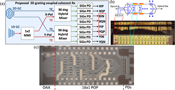
A coherent receiver using advanced digital signal processing was achieved for 100 Gbps dual-polarization QPSK transmission [48]. As shown in figure 2(a), integrated grating couplers, modified hybrid mixers, and high-speed Si-germanium (Ge) photodiodes were employed by the receiver. Polarization beam splitters and rotators needed in traditional coherent receivers were replaced by 2D polarization-splitting grating couplers [48].
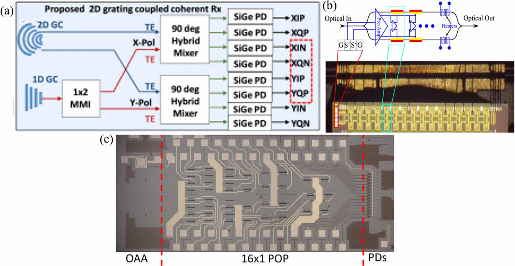
Figure 2 Schematic of integrated receivers for space communication. (a) Architecture of the receiver dual-polarization QPSK transmission. Reproduced from [48]. CC BY 4.0. (b) A wire bonded chip and block diagram of the fabricated MZM with a pre-amplifier and a distributed driver. Reproduced with permission from [51]. (c) Photograph of the fabricated Si photonics free space optical receiver. Reproduced from [52], with permission from Springer Nature.
Download figure:
Standard image High-resolution imageThe H2020-SPACE-ORIONAS project was an innovation action program funded by the European Commission to develop devices for new generation optical inter-satellite links. PICs explored by ORIONAS were used to considerably shrink the SWaP of lasercom terminals [49]. A self-configuring Si photonic receiver for space optical communication was supported by the European Commission through the H2020 project [50]. The receiver based on mode division multiplexing was employed to receive two spatially overlapped Hermite–Gaussian beams modulated at 10 Gbps. These two beams, sharing the same wavelength and polarization state, were separated with an isolation degree greater than 30 dB, and sorted out without introducing any excess loss or degradation in the transmitted signals. The network structure was composed of adjustable Mach Zehnder interferometers (MZIs) [50].
A monolithically integrated coherent receiver for O- and C-band funded by the H2020-SPACE-ORIONAS project was proposed to address the increasing demand for higher data rates and capacity [53]. The receiver featured a network of 2 × 2 multimode interference couplers as 90° optical hybrid. The total power consumption of the device was 460 mW with a chip size of approximately 6 mm2 and an optoelectronic bandwidth of 33 GHz. 64 GBd QPSK was demonstrated in O- and C-band. It was competitive to the Si-based coherent receiver in the C–band, and the highest symbol rate for O-band coherent communication [53].
In 2023, the Interuniversity Microelectronics Center funded by the European Space Agency reported a photonic receiver composed of 14 × 12 grating coupler arrays for satellite laser communication terminals [54]. The received optical signal was combined at an electrical circuit via integrated Ge photodiodes. The light-receiving area of the receiver was 200 µm × 200 µm. Considering the minimum efficiency of −10.5 dB, the receiving area was 95% of the designed receiver when illuminating by laser sources with mode field diameters from 20 µm to 300 µm [54].
The receiver shown in figure 2(b) presented the ability of reconfigurable and real-time orthogonal time-domain detection of a high-bandwidth Nyquist signal. All parameters were completely tunable in the electrical domain. The feasibility of the scheme was demonstrated through a proof-of-concept experiment over the entire C–band, employing a 24 Gbaud Nyquist QPSK signal [51].
A multi-aperture receiver shown in figure 2(c) was proposed to compensate the perturbation caused by atmospheric turbulence in free space optical communication systems [52]. The receiver sampled the distorted wavefront on different points and added the various signals coherently. The optical front-end of the receiver was entirely integrated in a Si photonic chip hosting a 2D optical antenna array and a self-adaptive analog programmable optical processor made of a mesh composed of tunable MZIs. The receiver enabled energy and cost-effective operation, scalability, modulation-format and data-protocol transparency, and pluggability with commercial fiber optics transceivers. The receiver demonstrated indoor free space optical transmission at a data rate of 10 Gbps [52].
High-performance receivers for optical communication possess advantages of high bandwidths, responsiveness, and quantum efficiencies, as well as low dark currents. To further improve the performance of the receiving chips, it is necessary to solve the heterogeneous integration between different materials, reduce nonlinearity effects of the detectors, improve receiver transmission rates, balance costs and power consumption. To mitigate the atmospheric turbulence in real time, multimode receivers based on spatial or modal diversity are promising architectures for much more robust to atmospheric turbulence. Mode diversity receivers provide higher collection efficiencies, low bit error ration, and much less synchronization losses. The number of modes considered for the multimode receiver should be chosen carefully. Optical mode diversity receivers based on a spatial demultiplexers and silicon photonic coherent combiners can also be used to reduce the atmospheric turbulence effects. For control electronics, PIC-based receiver would use FPGAs instead of switches for a fast detection of laser signals and higher integration/lower mass and volume.
2.2. Microwave photonic chips for space communicationMicrowave photonics utilizes photon technologies to generate, manipulate, transport, and process microwave signals. It possesses the advantages of low propagation losses, wide bandwidths, reconfigurability, low delays, and resistivity to electromagnetic interferences. Microwave photonic modules based on discrete devices, which are sensitive to external perturbations, cannot meet the requirements of practical applications in terms of stability, reliability, and costs. The generation of high throughputs of satellite telecommunication brings a huge impact on payload mass, volume and power consumption. Integrated microwave photonic systems play an important role in space communication with miniaturized devices to meet the increased capacity and performance demand.
Optical losses are important for microwave photonics systems for the quadratic translation. Many efforts were taken to reduce optical losses [55] at the early stages of integrated microwave photonics. Advanced functionalities and high-performance cooperating with integration have been the key of microwave photonics in recent years [28]. This section mainly involves electro-optic modulators, local oscillators, and filters in microwave photonics. Repeaters and mixers are introduced as well.
2.2.1. Electro-optic modulatorsOptical modulators are key components in microwave photonic chips. Microwave signals can be loaded onto optical signals by modulators for the wide bandwidth. Optical modulators are the first step in microwave photonics systems. The bandwidth, loss, linearity and dynamic range of the overall system are determined by optical modulators.
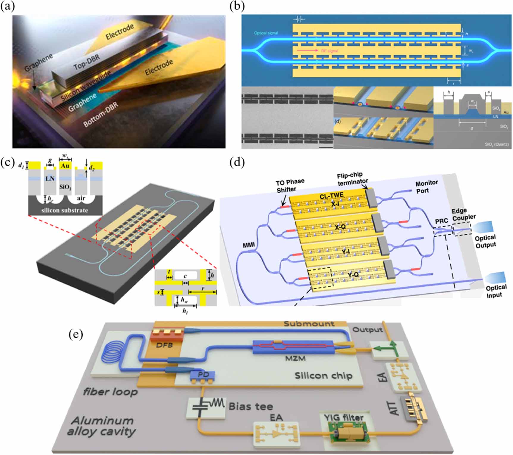
Electro-optic modulators are critical components of PICs to convert electrical signals to optical ones. Their performance is dictated by the response time, driving voltage, and physical footprint. All of these contribute to the component density and applications of PICs. A modulation speed of 60 GHz was achieved by a double-layer graphene modulator integrated on Si using vertically distributed Bragg reflector cavities (as shown in figure 3(a)) [56].
Figure 3 Typical microwave photonic modulators and local oscillators. (a) Schematic of the high-performance graphene optical modulator. Reproduced from [56]. CC BY 4.0. (b) A LiNbO3 modulator with segmented electrodes. Reproduced with permission from [57]. (c) Sketch of the ring modulator. Reproduced with permission from [58]. (d) Schematic of the dual-polarization in-phase quadrature modulator Reproduced with permission from [59]. (e) Schematic of the proposed hybrid-integrated wideband tunable optoelectronic oscillator. Reproduced with permission from [61].
Download figure:
Standard image High-resolution imageLiNbO3 modulators are widely used for the excellent electro-optic properties. A thin film LiNbO3 modulator based on segmented electrodes shown in figure 3(b) was used to achieve low-voltage and high-bandwidth modulation. Such a micro-structured electrodes broke the voltage-bandwidth limits in integrated LiNbO3 modulators and enabled sub-volt modulators with a bandwidth >100 GHz [57]. A thin film LiNbO3 modulator with a micro ring assisted MZI (as shown in figure 3(c)) demonstrated a modulation bandwidth greater than 67 GHz and a half-wave voltage length product of 0.35 V · cm [58]. The dual-polarization thin film LiNbO3 modulator shown in figure 3(d) achieved a bandwidth of exceeded 110 GHz and a record net data rate of up to 1.96 Tb s−1 [59]. The Si modulator based on cascaded distributed Bragg gratings realized a 110 GHz bandwidth with a 124 μm length [60].
2.2.2. Local oscillatorsLocal oscillators with high frequencies and low phase noise are important for microwave systems. The electrical signals can be generated using optical frequency combs or optoelectronic oscillators.
Local oscillators based on frequency combs come from the heterodyne detection approach. Two beams with different frequencies are usually required in the heterodyne detection. Photodetectors obtain the electrical signal corresponding to the frequency difference between the two beams. Due to the incoherent phase noise of the two beams, microwave signals with high noise are generated. Two optical filters were used by the frequency comb approach to generate microwave signals with eliminated phase noise.
A soliton microcomb and a semiconductor gain-switched comb were combined to demonstrate low-noise microwave generation. To derive an ultra-low noise microwave reference signal, a pump laser was used to generate a Kerr frequency comb with a repetition rate of 14 GHz. The phase noise at 10 kHz offset was below −135 dBc Hz−1 [62]. A microresonator with a quality factor of over 4 billion generated an 11 GHz soliton microwave source with an absolute phase noise of −133 dBc Hz−1 at a frequency offset of 10 kHz [63].
Optoelectronic oscillators generate microwave signals with high frequencies, broadband tenability, and ultra-low phase noise without microwave reference signals [61, 64]. A Si photonic chip and an electronic one were connected to the microstrip line through wire bonding. This hybrid integrated optoelectronic oscillator shown in figure 3(e) exhibited a broadband tuning range of 3–18 GHz. The phase noise of the microwave signal at 10 kHz offset could be as low as −128 dBc Hz−1 [61].
2.2.3. Microwave photonic filtersAs important components for reconfigurable radio frequency front ends of satellite communication, integrated microwave photonic filters (MPFs) are considered as a promising solution to overcome the inherent electronic limitations in bandwidths and flexibility. MPFs with widely tunable central frequencies (4–40 GHz) and tunable bandwidths (from 30 to 300 MHz) are required to meet the reconfigurable dynamic configuration after the launch of satellites. It is hard to meet these requirements for traditional electrical radio frequency filters [40]. Integrated MPFs can solve these problems.
According to the working mechanism, integrated MPFs can be mainly divided into structures based on microrings/microdisks [65, 66], microrings assisted MZI filters [67], the waveguide Bragg grating ones [68], frequency comb-based schemes [69], and stimulated Brillouin scattering filters [70]. The frequency comb-based scheme is limited in bandwidths and control complexity. Stimulated Brillouin scattering filters require an additional pump light source and cannot achieve high-density integration.
The principle of filters based on microring/microdisk resonators is to transform the frequencies of optical resonators to the microwave band through photoelectric conversion. Bandpass or band stop filtering functions can be achieved by microrings/microdisks-based MPFs. The bandwidth of a microring bandpass filter based on low loss Si3N4 waveguide was 113 GHz, the resolution of the signal processor was lower than 420 MHz, and the spurious free dynamic range was 112 dB·Hz2/3 [71]. An MPF including a high-speed phase modulator and a tunable high-Q micro-disk resonator demonstrated a passband of 1.93 GHz, a tunable range from 3 to 10 GHz, and an extinction ratio of 15 dB [66]. A notch filter based on cascaded micro ring resonators (MRRs) achieved a link gain of 8 dB, a noise figure of 15.6 dB, and a spurious free dynamic range of 116 dB·Hz2/3. A spectral resolution of 150 MHz and a stop band suppression ratio over 50 dB were simultaneously obtained by the MPF [65].
MRRs, racetrack resonators, and cascaded MRRs based on MZIs can be used to further improve the spectral resolution and rejection ratios of MPFs. A narrowband bandpass MPF with high selectivity is highly desirable in microwave photonic applications. A tunable MPF based on an ultrahigh quality factor Si MRR demonstrated a half width at half maximum of 170 MHz, a suppression ratio of 26.5 dB, and an operating frequency of 2–18.4 GHz [72]. As shown shown in figure 4(a), a Si-based MPF with flattop passband and adjustable bandwidths was realized by using a 10th-order MRR and a photodetector. The adjustable bandwidth of the MPF with flattop passband was from 5.3 to 19.5 GHz, and the rejection ratio exceeded 30 dB [73]. A reconfigurable bandwidth of 0.24–1.76 GHz was achieved by a microwave photonic bandpass filter using a coupled resonator optical waveguide and tunable coupling regions. The center wavelength tuning range and the rejection ratio were 4–36 GHz and 42.77 dB, respectively [74].
Figure 4 Typical integrated MPFs. (a) Optical micrograph of the fabricated filter with cascaded MRRs. Reproduced with permission from [73]. (b) Schematic diagram of the hybrid integrated MPF. Reproduced with permission from [78]. (c) Schematic of the Si IQ modulator-based MPF. Reproduced from [79]. CC BY 4.0.
Download figure:
Standard image High-resolution imageAn ultrahigh peak rejection exceeding 60 dB, a full width at half-maximum bandwidth of 780 MHz, and a frequency tuning range of 0–40 GHz were achieved by a SOI-based widely tunable microwave photonic notch filter. The MPF included an under-coupled MRR assisted by two cascaded tunable MZIs and three heaters [75]. Similar notch filters were implemented based on an MZI coupled Si3N4 MRR [76] and two cascaded Si MZIs coupled racetrack resonators [77].
The spectral characteristics of MRRs assisted MZI bandpass filters are determined by thermo-optic phase shifters and coupling strength between the MRR and the MZI arm. The tunable frequency ranges were ultimately determined by the free spectral ranges affected by the circumferences of the MRRs and the group indices of the waveguides. The first single-chip integrated microwave photonic low-pass filter on the InP platform implemented a free spectral range of 20 GHz and a 3 dB bandwidth for electro-optical transmission of 5.5 GHz. A maximum spurious dynamic range of 81.4 dB · Hz2/3 at a modulation frequency of 1.4 GHz was achieved as well [67].
Adjusting the center frequencies of each stage of the cascaded MRRs assisted MZIs structure was another way to control the bandwidths of bandpass filters. Compared with one-stage ring-assisted MZIs, the sideband suppression ratios could be further improved. The bandwidth of a reconfigurable rectangular filter based on three-stage cascaded ring-assisted MZIs could be tuned from 14.1 GHz to 4.1 GHz [80].
Bandstop and bandpass switchable MPFs based on integrated tunable dual rings coupled MZIs have been demonstrated. The center frequency and bandwidths of the switchable MPF were both reconfigurable. A filter with cascaded MRRs obtained a frequency tuning range of 4–25 GHz. Bandwidth tuning ranges of the passband and stopband MPFs were 4.5–9.7 GHz and 3.7–6.4 GHz, respectively. A rejection ratio about 20 dB was achieved [81].
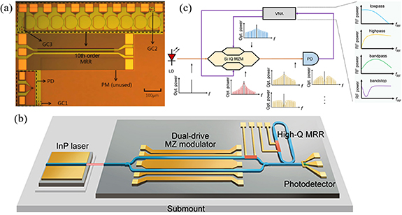
A high spectral resolution of 360 MHz, a tunable range from 3 to 25 GHz, and a large rejection ratio of >40 dB were exhibited by the all-integrated MPF with agilely switchable bandpass and band-stop function shown in figure 4(b) [78]. The all-integrated MPF was achieved through hybrid integration of an InP chip-based laser and a monolithic photonic circuit consisting of a dual-drive MZM, a high-Q ring resonator, and a photodetector. The bandpass and band-stop function could be agilely switched with a transient respond time of ∼48 μs. The spectral resolution was dramatically improved by nearly one order of magnitude. The valid frequency tunable range was broadened more than twice [78].
A robust MPF based on a single Si in-phase/quadrature modulator shown in figure 4(c) presented significantly improved temperature and carrier wavelength sensitivities [79]. Upconversion and the processing of signals were simultaneously realized by the MPF, that could be reconfigured as low-pass, high-pass, band-pass, or band-stop filters. The center frequency variation was within 0.2 GHz for the temperature range from 25 °C to 75 °C. For wavelength from 1500 to 1600 nm, the center frequency variation was within 2 GHz [79].
2.2.4. Repeaters and mixersTo realize broadband, highly integrated, and cost-effective communications satellite payloads, a massively multiplexed and high flexible signal processing module is highly desirable. A hybrid integrated microwave-photonic satellite repeater with large-scale multiplexing potential and high flexibility included an InP/Si3N4 external cavity laser, arrayed InP modulators, SOAs, and multifunctional Si3N4 signal processors. A Ka-band signal with a 3 dB bandwidth of 2 GHz was successfully downconverted into four 500 MHz sub-bands intermediate frequency signals [82].
Integrated microwave photonic mixers are very important for radio access networks, inter- and intra-satellite communications. Dual parallel single-drive MZMs and balanced detection were used in a Si photonic mixer [66]. As the first fully on-chip downconverter with electrical-in, electrical-out frequency conversion, a microwave photonic mixer achieved spur-free dynamic ranges >100 dB · Hz2/3, high gains, and low noise figures approaching 20 dB [83].
Significant progress has been made in the performance of integrated microwave photonic modules in recent years, but there are still gaps in key indicators such as link gains, noise coefficients, and spur-free dynamic ranges compared to discrete systems. Hybrid integration based on advanced packaging is a key link towards microwave photonics-based space communication. Hybrid integration based on multiple material platforms can also be used to improve performance of integrated microwave photonic chips. It is necessary to reduce losses of waveguides to achieve high-performance space communication based on microwave photonics. Photodetectors with high sensitivity, integrated optical amplifiers, and high-linearity optical modulators with low losses and high efficiencies are highly needed to achieve high-performance space communication with integrated microwave photonic chips.
In addition to satellite-based communication, space sensing is another important application of integrated photonics. Typical usage of integrated photonics in the field of space sensing are introduced bellow, which mainly involves light detection and ranging (LiDAR), devices for space imaging, inertial sensors, and spectrometers. Parameters such as distances and velocities can be obtained by ranging. Morphology information of objects can be shown by imaging. As a core component of inertial sensors, gyroscopes play a leading role in rotational angular velocity measuring and motion tracking of objects. Spectrometers are important instruments for material characterization and composition analysis. More details of the devices will be given in this section.
3.1. Integrated photonics for rangingAs a kind of real time remote sensing technology, LiDAR measures precise distances and movements of targets by emitting laser beams and processing echo signals. It can be typically divided into mechanical LiDAR and solid-state one. Mechanical LiDAR uses moving structures, such as motor-driven rotating stages or mirrors, to achieve beam scanning with a large range. However, it is bulky, complex, expensive, and possess low scanning speeds, poor accuracy and stability. It may be affected by impact vibrations from environment and mechanical wear during long-term operations. Solid-state LiDAR based on integrated optical phased arrays (OPAs) achieves stable, reliable, accurate, and fast chip-scale beam scanning. The concept of OPAs originates from microwave phased arrays. An antenna array with specific phase relationships among elements forms a beam in space and can be controlled by adjusting the phases.
The first Si-based integrated OPA achieved a field of view of 2.3° × 14.1° [84]. A 2D OPA densely integrated on a Si chip possessed a footprint of 0.58 mm × 0.58 mm. All the antennas were precisely balanced in power and aligned in phase to generate a designed, sophisticated radiation pattern in the far field [85]. The first fully-integrated OPA chip using the hybrid Si platform consisted of 164 optical components including lasers, amplifiers, photodiodes, phase shifters, grating couplers, splitters, and a photonic crystal lens. Beam scanning in the range of 23° × 3.6° with a beam width of 1° × 0.6° was exhibited by the OPA chip [86]. An OPA with a flat interference zone based on high-contrast grating antennas presented in figure 5(a) was used to achieve greatly enhanced emission efficiency in a broad wavelength range [87]. The proposed structure worked as a whole device and achieved beam steering without crosstalk. The 16-channel OPA enabled a field of view of 45.6° × 20.2° and a beamwidth of 2.4° × 2.5° [87].
Figure 5 Typical OPA chips. (a) A high contrast grating antenna-based OPA with high efficiency and low crosstalk. Reproduced with permission from [87]. (b) A Ⅲ–V/Si OPA. Reproduced with permission from [92]. (c) A Si/Si3N4 dual-layer OPA. Reproduced with permission from [93]. (d) Schematic of a serpentine OPA. Reproduced with permission from [94].
Download figure:
Standard image High-resolution imageThe field of view of a periodic OPA is limited by sidelobes. Non-uniform OPAs were proposed to suppress sidelobes. An OPA chip with non-uniform spacing simultaneously achieved a wide steering angle of 80° × 17° and more than 60 000 resolvable points in 2D beam scanning [88].
A 16-channel end emitting OPA with a SiO2 cavity at the front end presented a flat far-field envelope within a 64° field of view [89]. A 32-channel OPA without optical crosstalk between waveguides could perform beam scanning within ±45° [90]. A waveguide superlattice-based OPA chip presented a field of view of 180° [91].
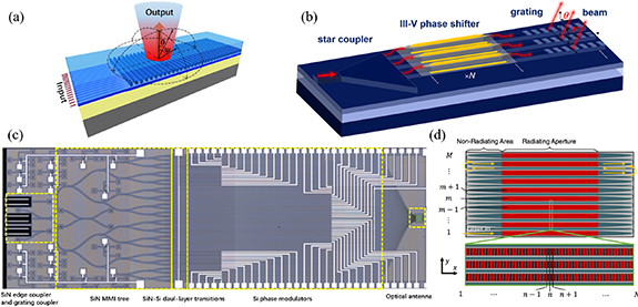
Modulation effects in Ⅲ–V/Si phase shifters can be used to increase modulation efficiencies and decrease operating voltages. The Ⅲ–V/Si phase shifter with higher electron mobility decreases carrier absorption loss and potentially allows for low residual amplitude modulations and high-speed operations. An OPA illustrated in figure 5(b) consisted of a star coupler, Ⅲ–V/Si phase shifters, and grating antennas [92]. The 4 µm-pitch heterogeneous phase shifters in the OPA enabled V2π of only 0.35–1.4 V across 200 nm, low residual amplitude modulation of only 0.1–0.15 dB for a 2π phase shift [92].
Due to the strong nonlinear
Comments (0)